Activity 5 Part (b): Frequency Response Identification of a Boost Converter Circuit

Key Topics: Frequency Response Analysis, System Identification, Nonlinear Systems, Pulse-Width Modulation, Bode Plots
Contents
Equipment needed
- Arduino microprocessor (e.g. Uno, Mega, etc.)
- Breadboard
- Battery (AA for example)
- Electronic components (inductor, resistor, capacitor)
- Diode
- Transistor (MOSFET)
- Jumper wires
The system we will be employing in this activity is a type of DC/DC converter called a Boost (Step-Up) Converter. The purpose of a boost converter is to take the voltage supplied by a constant voltage source (e.g. a battery) and output an (approximately) constant higher output voltage. Details regarding the principle of operation of a boost converter can be found in Part (a) of this activity. We will implement a couple of very simple (not optimized) versions of a boost converter in order to illustrate how to experimentally determine the frequency response of a system. In this part of the activity, the Arduino board will be used for measuring the output of the circuit via one of the board's Analog Inputs and for controlling the level of the output voltage via one of the board's Digital Outputs. The Arduino board will also communicate the recorded data to Simulink for visualization and analysis.
A schematic of the boost circuit we will analyze in this section is shown below including a list of the variables we will employ.
(Rload) resistance of the load resistor
(Req) equivalent series resistance (ESR) of the inductor
(L) inductance of the inductor
(C) capacitance of capacitor
(ei) input voltage (from the battery)
(eo) output voltage

Purpose
The purpose of this activity is to build further intuition regarding the operation of a boost converter circuit. Specifically, in this part of the activity we will model the circuit based on experimentally obtained frequency response data. This technique provides intuition regarding frequency response analysis and demonstrates a blackbox approach for generating an approximate (local) model of a nonlinear system.
Frequency response experiment
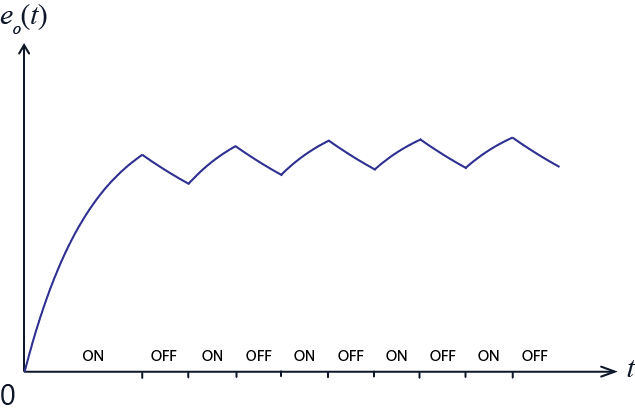
Referring to the analysis of Part (a) of this activity, we demonstrated that the output voltage of the boost circuit chatters up and down as the transistor (MOSFET) is switched on and off as shown in the following. The output, however, can approximate a constant (DC) voltage by employing a very high switching frequency and by including a capacitor to "filter" the ripple.
One of the challenges of designing a controller for a DC/DC converter is that the plant model is inherently nonlinear due
to the switching between the two discrete states of the circuit. One solution to this challenge is to generate a linear model
that averages the ON and OFF states of the boost converter in order to approximate the true nonlinear behavior of the circuit.
This approach is appropriate when the switching frequency is sufficiently high such that the chatter in the output voltage
is small and can be well approximated by a single continuous model. In practice, the averaged model removes the switch and
employs an equivalent inductance in place of the true inductance. Often the equivalent inductance is modeled in terms of the
duty cycle  as
as  . If the converter operates in a small range of duty cycles, then employing a constant
  in the model is appropriate.
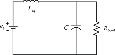
Below is shown a depiction of an averaged boost converter model. Here we have neglected the equivalent series resistance for
the inductor since in practice it is often negligible in comparison to other effects. Often a resistance  is included in series with the capacitor to better model the impedance of the capacitor for high frequency switching inputs,
though we have not done so here.
So far we have analyzed the boost converter for an input of  and an output of
  . In practice, our control input to the converter is actually the duty cycle, that is, the percent of time the converter switch
is on. With this in mind, we can generate the following linearized model of the averaged boost converter shown above. This
transfer function has for its input the deviation
  of the current duty cycle
  from some nominal duty cycle
  , that is,
  . Similarly, the output is the deviation
  of the output voltage
  from the nominal output voltage
  that corresponds to the nominal duty cycle
  , that is,
  .
.
(1)
The above model is helpful in providing some insight into the behavior of the boost converter. Specifically, we can see the system has two poles due to the LC filter inherent in the circuit. Also interesting is that the model has a non-minimum phase zero. The behavior of a non-minimum phase system such as this is characterized by the fact that its response to a step input initially moves in a direction opposite of the commanded direction. In this case, this means that an increase in duty cycle will initially cause the output voltage to drop before beginning to increase toward its ultimate steady-state value. The intuition behind this behavior is as follows. An increase in duty cycle means that the circuit is in its ON state for a longer period of time. In the ON state, the current from the battery will flow through the switch and the load is in essence disconnected from the battery for a longer period of time. Therefore, the output voltage will initially drop. This increased ON time also, however, causes the current through the inductor to rise. This increase in current through the inductor eventually leads to an increase in output voltage.
Despite the intuition provided by the model given above, its accuracy may be limited. For example, inaccuracies in the model could be due to failing to capture the non-ideal nature of the circuit components, as well as failing to capture the dynamics of the channels of the Arduino board which are inherently part of our closed-loop system. One solution is to generate a blackbox model of the boost converter based on empirical data. Specifically, a common industrial practice is to experimentally generate a frequency response model of the boost converter. We will do that here by experimentally generating a Bode plot of the boost converter's frequency response.
Hardware setup
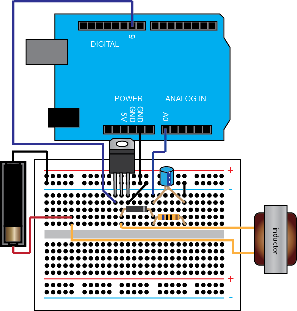
Our hardware setup will be exactly the same as that employed in Part (a) of this activity, except we will use different value components for the capacitor and the load in order to make the boost
circuit respond faster. Specifically, we will employ a 1200  capacitor and a 1000
  resistor for the load. Furthermore, we will still use a Digital Output of the Arduino board to switch our transistor, but
in this case we will use a hardware-generated PWM signal. Only those Digital Outputs marked by the ~ symbol can generate such
a PWM signal. The frequency of the hardware-generated PWM is constant and much faster than what we can achieve in software
with Simulink. Most pins generate a PWM signal with an approximate frequency of 490 Hz. On the Arduino Uno and some similar
boards, pins 5 and 6 generate a PWM signal with a higher frequency of 980 Hz.
Looking at the theoretical linear averaged boost converter model given above with denominator  , we expect the system to have a natural frequency of
  . For our circuit components and a 1.5-Volt battery with nominal duty cycle of 0.39, we expect that the natural frequency
of the boost converter to be around 17.6 rad/sec (
 2.80 Hz). Since we expect the magnitude of the boost converter to begin to roll off around this frequency (it will begin
to attenuate inputs with frequencies above this threshold), the hardware-generated PWM signal should be sufficiently fast.
In other words, since 490 Hz is more than two decades larger than 2.80 Hz, the boost circuit should in essence filter the
square wave input resulting in a relatively smooth output voltage.
Software setup
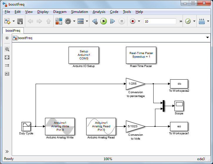
Our Simulink model for performing this frequency response experiment will be similar to our model from Part (a) of this activity. In order to trigger the hardware generated output, we will replace the Digital Write block with the Analog
Write block from the IO package. For details on how to use the IO package, refer to the following link. The name of the Analog Write block is a bit of a misnomer since the output is still digital, but the block does generate
the PWM signal we desire. The desired duty cycle is specified as an 8-bit number. Since  , the block accepts inputs between 0 and 255 where 0 corresponds to a
  duty cycle and 255 corresponds to a
  duty cycle. We will continue to use Pin 9 for our digital output. We will also replace the Pulse Generator block with a Sine Wave block from the Sources library since
frequency response data is generated from the system's response to sinusoidal inputs over a range of frequencies. For the
Sine Wave block, we will continue to employ a Sample time of Ts that has been set to 0.01 seconds. Furthermore, we will set the Bias to "100" and the Amplitude to "40". Therefore, the Sine Wave block will generate a sinusoid that varies between 60 and 140, which corresponds to the
duty cycle varying between approximately
  and
and  . The frequency of the Sine Wave will be varied throughout the experiment. A depiction of the modified Simulink model is shown
below and can be downloaded here.
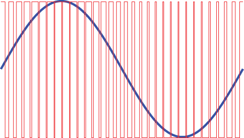
It can be a little difficult to envision the physical input to our system. The following figure may help by illustrating how the duty cycle is changing sinusoidally. The input signal is still the digital PWM signal, but the percent of time the PWM signal is "ON" is changing smoothly.
Bode plot generation
With frequency response analysis we are interested in examining how a system responds to different frequency sinusoidal inputs. For linear (or locally linear) systems, we know that in steady state a sinusoidal input will generate a sinusoidal output of the same frequency, but with possibly different amplitude and phase. It is this scaling of the amplitude and time shifting that we are interested in. We will experimentally determine this scaling (magnitude) and phase information, then we will represent the information in the form of a Bode plot.
Setting the frequency of the Sine Wave in our Simulink model to  rad/sec (1 Hz) and running the model, we generate the following output voltage response demonstrating how our 1.6-Volt battery
input can be stepped to a higher voltage depending on the control of the transistor switching.
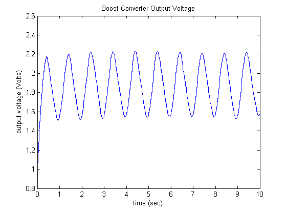
Examining the above, we can see that there is an initial transient due to the natural response of the circuit, but once that dies out, the steady-state response exhibits the sinusoidal response we expected. Assuming that the To Workspace blocks in our Simulink model are set to have Array outputs, the following MATLAB commands will plot the steady-state voltage output (starting at 3 seconds) on the same set of axes as the duty cycle input, thereby demonstrating the resultant scaling and shifting of the output.
         [AX,H1,H2] = plotyy(3:0.01:10,eo(301:1001),3:0.01:10,dc(301:1001),'plot');
         xlabel('time (sec)')
         set(get(AX(1),'Ylabel'),'String','output voltage
         (Volts)')
         set(get(AX(2),'Ylabel'),'String','duty cycle')
         title('Boost Circuit Frequency Response (freq = 1 Hz)')
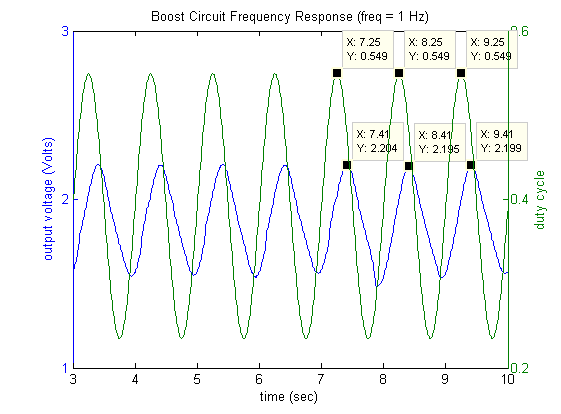
From the recorded data shown above, we can calculate the magnitude and phase response of our boost converter at this frequency,
 rad/sec. First we will estimate the magnitude. We know that the input duty cycle sinusoid has an amplitude of 40/255
  0.16. From inspection of the output voltage data, the difference between a peak and the valley that immediately succeeds
it is on average approximately 0.66 Volts which corresponds to an amplitude of 0.66/2 = 0.33 Volts. We use only successive
peaks and valleys for determining amplitude because the bias in the output can drift. Based on these two observations, the
magnitude of the boost converter at this frequency is 0.33/0.16
  2.06. When converted to decibels, the magnitude at this frequency is 20
  2.06
2.06  6.28 dB. Next we will estimate the phase. From inspection of the above, we can see that the output lags behind the input
(as expected). Comparing a peak of our input duty cycle signal to the peak of the output voltage signal that immediately follows
it, we can see that the output signal is shifted by on average 0.16 seconds (note that the frequencies of the input and the
output are equal (1 Hz)). Since the period of our signals are 1 second, that means our output lags behind the input by about
 of a cycle, where one cycle corresponds to 360 degrees (
 of 360 degrees
  58 degrees). Also, we use the convention that the phase is negative when the output lags behind the input. Calculating the
phase in a different manner, we can multiply the time lag by the frequency. Therefore, the phase lag is -0.16 seconds
  radians/second, which is approximately -1.0 radians. Converting to degrees, we again have that the phase is approximately
-58 degrees.
These calculations provide the frequency response of our boost converter at one frequency. If we repeat this process over a range of frequencies, we can experimentally create a Bode plot for our boost converter (for this set of conditions). Below is given a table of calculated magnitude and phase values for our boost circuit. This data is generated for a slightly different set-up than we have used so far, but the results are very similar to what would be generated for the original set-up. Specifically, the load resistor, capacitor, and inductor are unchanged, but we employed a different transistor and diode, and used a pin with the 980 Hz PWM signal. The transistor employed was an IRFZ44N Power MOSFET and the diode was an NTE585 Schottky diode. These components provide higher performance, but aren't really necessary for the level of power and PWM frequencies we are employing.
| Frequency (Hz) | 0.01 | 0.05 | 0.1 | 0.2 | 0.25 | 0.5 | 1 | 2.5 | 5 |
| Frequency (rad/sec) | 0.0628 | 0.314 | 0.628 | 1.26 | 1.57 | 3.14 | 6.28 | 15.7 | 31.4 |
| Magnitude (dB) | 9.52 | 9.35 | 9.06 | 9.16 | 8.96 | 7.44 | 6.15 | -0.28 | -9.83 |
| Phase (degree) | -0.36 | -0.00 | -0.36 | -5.76 | -9.0 | -28.8 | -75.6 | -90.0 | -162 |
This data can then be compiled in the form of a Bode plot by executing the following commands at the MATLAB command line.
freq  = [0.0628 0.314 0.628 1.26 1.57 3.14 6.28 15.7 31.4];
mag   = [9.52 9.35 9.06 9.16 8.96 7.44 6.16 -0.28 -9.83];
phase = [-0.36 0 -0.36 -5.76 -9 -28.8 -75.6 -90.0 -162];
subplot(2,1,1);semilogx(freq,mag,'*')
grid on
xlabel('frequency (rad/sec)')
ylabel('magnitude (dB)')
title('Boost Converter Empirical Bode Diagram')
subplot(2,1,2);semilogx(freq,phase,'*')
grid on
xlabel('frequency (rad/sec)')
ylabel('phase (deg)')
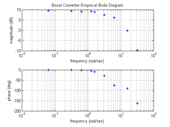
Examining the above Bode diagram, the frequency response of the circuit doesn't exactly agree with the theoretical linear averaged model given at the beginning of this section, but it does exhibit the same character. Specifically, the empirically-derived Bode diagram reflects a type 0 system with two poles, though the DC gain and the location of the poles are somewhat different than predicted by the theoretical linear averaged model. The system is type 0 because the magnitude plot is flat at low frequencies and the phase approaches 0 degrees at low frequencies. The presence of the two poles is indicated by the magnitude plot rolling off at a slope of approximately -40 dB/decade (and the phase appears headed towards -180 degrees). The contribution of the non-minimum phase zero cannot be seen because it is thought that its break frequency (around 160 rad/sec) is beyond the frequency band in which we can clearly identify the boost converter's response. This non-minimum phase zero would in theory add another 90 degrees of phase lag at high frequencies.
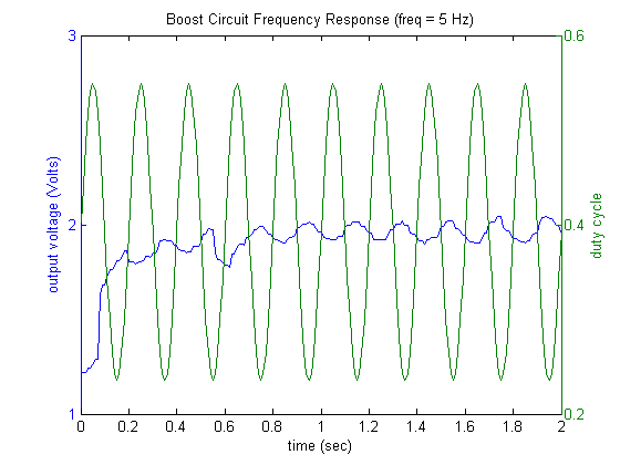
It is typical that the high-frequency behavior of a system is difficult to identify experimentally. This arises due to a couple of issues that can be illustrated by our physical experiment. One issue is that for physical systems the output tends to get attenuated at high frequencies. The following figure shows the 5 Hz data from our experiment which was the highest frequency we attempted to identify. At this frequency, we can already see that the amplitude of the output is getting quite small. As the amplitude becomes small, the various sources of error can become quite large as a percentage of the signal amplitude. For example, you can see that the quantization due to our analog-to-digital conversion is already significant and will become more so at even higher frequencies. The other issue is that at high frequencies the period of one cycle becomes quite small. Therefore, any errors in timing become a larger percentage of a single cycle. Again examining the following figure, one can see that the number of samples we are able to take per cycle is getting smaller (at 5 Hz, can sample about 20 times per cycle at most).
Even though the accuracy of our model is lacking at higher frequencies, it is often okay because we wouldn't wish to operate our boost converter in that frequency band anyway. It is, however, imperative that we understand what range of frequencies of input commands we can achieve for our given system.
Extensions
Some extensions to this activity would be to experiment with different circuit components to see what kind of performance can be achieved. It could also be interesting to examine other types of DC/DC converters, such as the buck converter and the buck-boost converter. In Part (c) of this activity, we will design and implement a controller for maintaining the output voltage of the boost converter we examined here.


