Activity 5 Part (c): Feedback Control of a Boost Converter Circuit

Key Topics: Frequency Response Analysis, System Identification, Lead Compensation, Embedded Control, Autocode Generation
Contents
Equipment needed
- Arduino microprocessor (e.g. Uno, Mega, etc.)
- Breadboard
- Battery (AA for example)
- Electronic components (inductor, resistor, capacitor)
- Diode
- Transistor (MOSFET)
- Jumper wires
The system we will be employing in this activity is a type of DC/DC converter called a Boost (Step-Up) Converter. The purpose of a boost converter is to take the voltage supplied by a constant voltage source (e.g. a battery) and output an (approximately) constant higher output voltage. Details regarding the principle of operation of a boost converter can be found in Part (a) of this activity. The frequency response behavior of a boost converter is studied in Part (b) of this activity. In this part of the activity, we will implement a control system in order to control the output voltage of the converter circuit. Such a control system is necessary if it is desired to change the output voltage setpoint, or if the system conditions change (e.g. input voltage source changes, load changes, etc.). In particular, we will use a frequency response approach to design the feedback controller. In this activity, the Arduino board will be used for measuring the output of the circuit via one of the board's Analog Inputs and for controlling the level of the output voltage via one of the board's Digital Outputs. The Arduino board will also communicate the recorded data to Simulink for visualization and analysis. The control logic will be specified within Simulink and initially the controller will run on-board the host computer. Eventually we will target this control logic to the microprocessor on the Arduino board.
A schematic of the boost circuit we will control in this section is shown below including a list of the variables we will employ.
(Rload) resistance of the load resistor
(Req) equivalent series resistance (ESR) of the inductor
(L) inductance of the inductor
(C) capacitance of capacitor
(ei) input voltage (from the battery)
(eo) output voltage

Purpose
The purpose of this activity is to demonstrate how to design a controller using frequency response techniques based on an empirically derived, and imperfect, plant model. Furthermore, this activity demonstrates how embedded controllers are often designed and implemented in practice using modern design and code generation tools.
Data-driven plant model
Referring to the analysis of Part (b) of this activity, we experimentally collected frequency response data from the boost converter circuit. Specifically, for
a duty cycle input that was sinusoidally varied about a nominal duty cycle of approximately 0.39, we observed the scaling
and phase shift of the output voltage signal. Using the following set of components: 1-H inductor, 1200-  capacitor, 1000-
  load resistor, IRFZ44N Power MOSFET, and NTE585 Schottky diode, we collected the following set of frequency response data.
| Frequency (Hz) | 0.01 | 0.05 | 0.1 | 0.2 | 0.25 | 0.5 | 1 | 2.5 | 5 |
| Frequency (rad/sec) | 0.0628 | 0.314 | 0.628 | 1.26 | 1.57 | 3.14 | 6.28 | 15.7 | 31.4 |
| Magnitude (dB) | 9.52 | 9.35 | 9.06 | 9.16 | 8.96 | 7.44 | 6.15 | -0.28 | -9.83 |
| Phase (degree) | -0.36 | -0.00 | -0.36 | -5.76 | -9.0 | -28.8 | -75.6 | -90.0 | -162 |
This data can be compiled in the form of a Bode plot by executing the following commands at the MATLAB command line.
freq  = [0.0628 0.314 0.628 1.26 1.57 3.14 6.28 15.7 31.4]; % frequency in rad/sec
mag   = [9.52 9.35 9.06 9.16 8.96 7.44 6.16 -0.28 -9.83];   % magnitude in dB
phase = [-0.36 0 -0.36 -5.76 -9 -28.8 -75.6 -90.0 -162];    % phase in degrees
subplot(2,1,1);semilogx(freq,mag,'*')
grid on
xlabel('frequency (rad/sec)')
ylabel('magnitude (dB)')
title('Boost Converter Empirical Bode Diagram')
subplot(2,1,2);semilogx(freq,phase,'*')
grid on
xlabel('frequency (rad/sec)')
ylabel('phase (deg)')
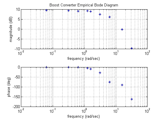
The above plot serves as an approximate model for our boost converter circuit in the neighborhood of the operating conditions that the experiment was performed for. We will use this data in designing a compensator for the boost converter circuit. Since it is more convenient to have an actual transfer function (or differential equation) model to employ in design, we will attempt to fit a mathematical model to this data.
The empirically-derived Bode diagram reflects a type 0 system with two poles. The system is type 0 because the magnitude plot
is flat at low frequencies and the phase approaches 0 degrees at low frequencies. Specifically, the low frequency portion
of the magnitude plot approaches approximately 9.5 dB which corresponds to a DC gain of approximately 3 since 20  3
3  9.5. The presence of the two poles is indicated by the magnitude plot rolling off at a slope of approximately -40 dB/decade
(and the phase appears headed towards -180 degrees). By some trial and error, it appears that the poles break somewhere in
the neighborhood of 10 rad/sec, which gives us an estimate of
  where we will assume that the two poles are complex conjugates of one another. Since the frequency response data does not
show a resonant peak, the magnitude does not increase in the neighborhood of the break, we can assume that the damping ratio
 is greater than 0.707. By trial and error, choosing
  0.9 seems to match the data pretty well. Therefore, we will assume the following for our plant model.
(1)
Using the system identification toolbox
Alternatively, if you have access to the System Identification Toolbox for MATLAB, there are commands that numerically fit a model to the frequency response data that we have generated. Specifically,
you can use the tfest command to fit a transfer function model to the our data represented in the frequency response data (frd) format (magnitude  and phase
  represented as a complex number
  ). The commands given below will return an estimated transfer function model with two poles
  and no zeros
  .
.
freq  = [0.0628 0.314 0.628 1.26 1.57 3.14 6.28 15.7 31.4];          % frequency in rad/sec
mag   = 10.^([9.52 9.35 9.06 9.16 8.96 7.44 6.16 -0.28 -9.83]/20);   % magnitude
phase = [-0.36 0 -0.36 -5.76 -9 -28.8 -75.6 -90.0 -162]*pi/180;      % phase in radians
resp = mag.*exp(i*phase);                                            % response as complex numbers
sys = frd(resp,freq);                                                % frequency response data
np = 2;                                                              % number of poles in model
nz = 0;                                                              % number of zeros in model
Ptb = tfest(sys,np,nz)                                               % estimated transfer function model
Ptb =

          369.2
  ---------------------
  s^2 + 24.66 s + 129.9

Continuous-time identified transfer function.

Parameterization:
   Number of poles: 2   Number of zeros: 0
   Number of free coefficients: 3
   Use "tfdata", "getpvec", "getcov" for parameters and their uncertainties.

Status:
Estimated using TFEST on frequency response data "sys".
Fit to estimation data: 77.39% (simulation focus)
FPE: 0.1526, MSE: 0.1209
Examination of the above model generated by the tfest command shows a relatively similar solution to the one we roughly estimated from inspection of our frequency response data. Alternatively, one can generate a fitted model using the System Identification Tool GUI which can be launched from the command line with the command ident.
Executing the following MATLAB commands demonstrate the agreement between the experimentally acquired magnitude data and the two models generated above.
K = 3;
wn = 10;
zeta = 0.9;
s = tf('s');
P = K*wn^2/(s^2 + 2*zeta*wn*s + wn^2);
freq  = [0.0628 0.314 0.628 1.26 1.57 3.14 6.28 15.7 31.4]; % frequency in rad/sec
mag   = [9.52 9.35 9.06 9.16 8.96 7.44 6.16 -0.28 -9.83];   % magnitude in dBs
phase = [-0.36 0 -0.36 -5.76 -9 -28.8 -75.6 -90.0 -162];    % phase in degrees
figure;semilogx(freq,mag,'r*')
hold;
O = bodeoptions;
O.PhaseVisible = 'off';
O.Xlim = [10^-2 10^2];
bodeplot(P,O);
bodeplot(Ptb,O,'r--');
grid on
legend('sight model','toolbox model')
xlabel('frequency (rad/sec)')
ylabel('magnitude (dB)')
title('Boost Converter Magnitude Data')
Current plot held
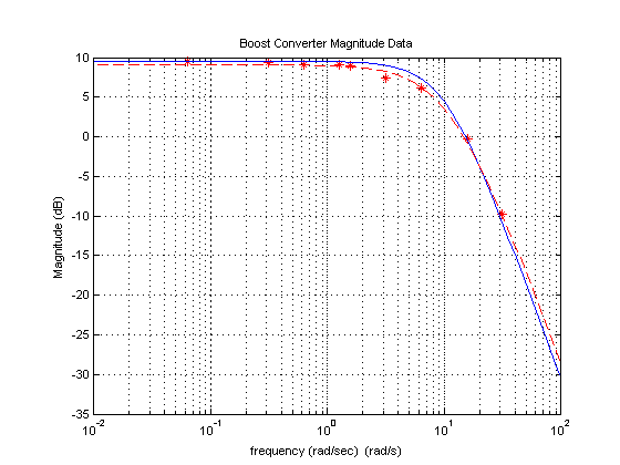
Similarly, we can examine the agreement for the phase data by adding the following additional commands.
O = bodeoptions;
O.PhaseVisible = 'on';
O.MagVisible = 'off';
O.Xlim = [10^-2 10^2];
figure;bodeplot(P,O);
hold;
bodeplot(Ptb,O,'r--');
semilogx(freq,phase,'r*')
grid on
legend('sight model','toolbox model')
xlabel('frequency (rad/sec)')
ylabel('phase (deg)')
title('Boost Converter Phase Data')
Current plot held
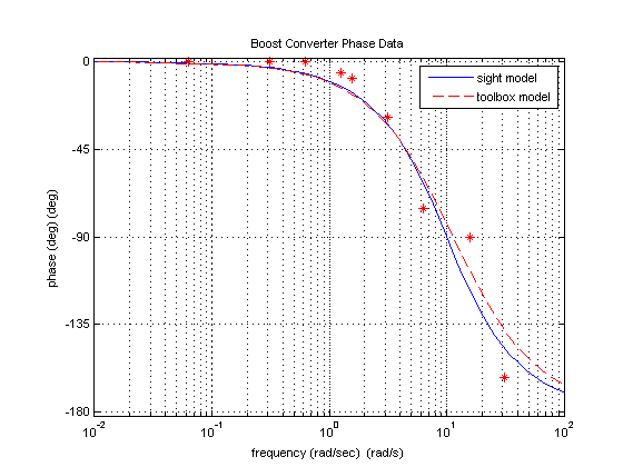
The relative accuracy shown in the above figures gives us some confidence that the extracted models of the plant given above will be suitable for control design purposes. Note, however, that as our data is limited to frequencies below 31.4 rad/sec, we will need to be careful regarding the behavior of our system at higher frequencies since our model is essentially unknown at frequencies much above 31.4 rad/sec.
Feedback control (static compensation)
At this point, we will implement a control system for the boost converter circuit. Specifically, we will implement what is termed a Voltage Mode Controller for the DC/DC converter where we command a setpoint for the desired level of output voltage and then feed back a measurement of the output voltage for use by our controller. A block diagram that conceptually represents this approach is shown below.

If the operating conditions were constant and sufficient testing could be done ahead of time, one could implement an open-loop controller where the testing has revealed what duty cycle input is needed to generate a corresponding output voltage in steady-state. Such an approach is likely not very robust since the plant and operating conditions may change frequently and/or aren't known well. For example, the input voltage source could change (battery voltage decreases with use, source could be a generator, etc.) or the load could change (load could age, torque could be applied to the motor being fed by the converter, etc.).
Hardware setup
Our hardware setup will be similar to that employed in Part (b) of this activity. Specifically, we will use the following set of components: 1-H inductor, 1200-  capacitor, 1000-
  load resistor, IRF1520 Power MOSFET, and 1N4007 diode. Furthermore, we will still use a hardware-generated PWM signal from
the Arduino board. We will use a 980 Hz PWM output (which is generated on pin 5 or 6 of most Arduino boards). An Analog Input
of the Arduino board will be used to measure the output voltage for use by our feedback controller.

One difference in hardware usage that will arise later is that we will employ the Arduino board for running the control logic. The physical connections and components will, however, remain unchanged. For now, we will run our control logic on board the host computer.
Software setup
Our Simulink model for performing this closed-loop Voltage Mode Control system will be similar to our model from Part (b) of this activity. We will still employ the blockset from the IO package for interfacing with the Arduino board, further details
can be found here. We will, however, add the logic for a feedback controller into our model. To begin, we will assume a simple proportional
controller with gain  and will attempt to track a step change in the desired output voltage setpoint. Specifically, the desired setpoint will begin
at 1.8 Volts before stepping to 2.8 Volts after 3 seconds. A depiction of the modified Simulink model is shown below and can
be downloaded here. The layout of this model makes the feedback structure of the control system quite clear. You can imagine that the plant
being controlled, the boost converter, is physically located between the Analog Write block and the Analog Read block. The
Analog Write block sends the PWM signal out into the physical world and the Analog Read block records the plant output and
brings it back into the control software. Inspection of the provided model reveals that the controller acts on the error in
deviation of the output voltage from some nominal level, that is, the error in
  . Furthermore, the controller generates a duty cycle command that is a deviation from the duty cycle that corresponds to
the nominal output voltage
  . The controller is set up this way because the plant model that we are employing for design was linearized about this nominal
output voltage (1.8 Volts) corresponding to a duty cycle of approximately 39 percent (100/255). In this instance, the controller
can be considered as only acting to correct deviations from the nominal operating point. Since the actual physical boost converter
accepts duty cycle as the input and generates an output voltage
  , we then must subtract the nominal voltage from the feedback signal to generate
  and we must add the nominal duty cycle to the output of the controller in order to supply the converter with the full duty
cycle command,
  .
.

It is worth taking a minute to think about what  represents in this model.
  is a constant equal to 0.5 that takes a voltage error as an input and produces a duty cycle command to the converter circuit.
Therefore,
  has units of percent/Volts and a 1-Volt error will generate a 50 percent change in the duty cycle command (away from the
nominal operating point). The conversion on the output of the Analog Read block converts the 10-bit number representing the
output voltage into units of Volts, while the conversion prior to Analog Write block converts the duty cycle command from
a percentage into an 8-bit number. The saturation block accounts for the fact that the duty cycle cannot be less than 0 (off
100 percent of the time) and cannot be greater than 1 (on 100 percent of the time). A proportional controller is by definition
Static since the relationship between the input and output doesn't change; a particular input will always produce the same output
from a static controller, no matter the conditions or history experienced by the system.
In the downloadable version of the model, the sample time of the various blocks is set to a variable Ts or is inherited. Defining the sample time as Ts = 0.02 at the MATLAB command line and running the model generates the following response.
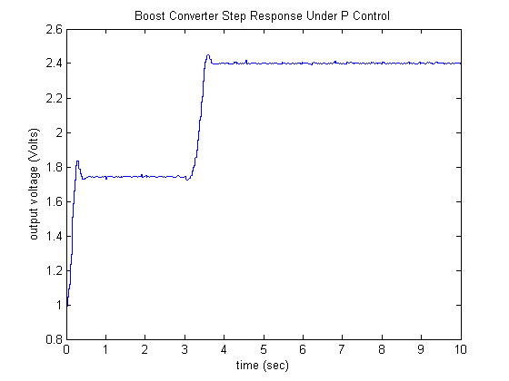
The closed-loop system reacts to being "turned on" at time  equal 0 seconds with the setpoint reference initially set to 1.8 Volts (though there may some initial charge on the capacitor
within the circuit). Then at 3 seconds the reference steps up to 2.8 Volts. Examination shows that the response is relatively
fast, is somewhat underdamped in that it exhibits overshoot, and eventually settles to a steady-state value that is offset
from the reference command of 2.8 Volts. The resulting non-zero steady-state error is expected based on the controller and
plant model we are assuming, which correspond to a unity-feedback system that is Type 0 (includes no integrators). Most controllers for DC/DC converters will add an integrator to increase the system type and reduce
the steady-state error to zero for a constant reference. We will develop such a controller in the following section.
Feedback control (dynamic compensation)
In this section we will develop a more sophisticated compensator for the boost converter circuit. As explained in the previous section, we proposed adding an integrator to our controller in order to increase the system type and drive the steady-state error to zero for a constant (DC) reference. The challenge with the addition of the integrator is that it adds 90 degrees of phase lag. This can de-stabilize the closed-loop system, especially if we would like to speed up the response of the system by pushing the gain crossover frequency higher. Therefore, we will add lead compensation to our integrator to help speed up the response and to compensate for the phase lag from the integrator. Since in practice a lead compensator cannot add more than about 70 degrees of phase lead, we will in fact employ two lead compensators such that our overall control will have the following form.
(2)
The presence of  -terms in our controller indicate that this is a dynamic compensator. Recalling that multiplication by
  corresponds to differentiation and division by
  corresponds to integration, one can see that the output of this compensator does not depend only on the current input, but
also past inputs (integration) and future inputs (differentiation). Such a compensator is Dynamic because the relationship between the current input and output changes with time.
In addition to achieving zero steady-state error, we will also attempt to design our compensator to achieve a sufficient amount
of phase margin (provides robustness, minimal overshoot) and to achieve as high a gain crossover frequency as possible (provides
speed of response). Specifically, we will attempt to achieve a phase margin of approximately 60 degrees and a gain crossover
frequency of 20 rad/sec. In terms of speed of response, one limit is that we need the gain crossover frequency  to be at least a decade or two below the PWM frequency in order to sufficiently "filter" the switching between the ON and
OFF states of the converter. In this case, we will aim for a crossover frequency of 20 rad/sec because it is well below the
PWM frequency and because it is just above the resonant frequency of the plant (the phase lag contributed by the plant hasn't
gotten too large yet). Recall the (simplified) model of the plant that we estimated from the experimentally generated Bode
plot:
(3)
The Bode diagram of the plant model with integrator is shown below. Inspection of the figure indicates that at the desired
gain crossover frequency of 20 rad/sec, the plant with integrator has a phase of -220 degrees. Therefore, in order to achieve
a phase margin of 60 degrees, corresponding to a phase of -120 degrees, the controller  needs to provide approximately 100 degrees of additional phase.

Since a single lead compensator cannot achieve 100 degrees of phase lead, we will employ two lead compensators where each one will provide approximately 50 degrees of phase lead. This desired level of phase lead determines the ratio between the zero and the pole of each lead compensator as shown below.
(4)
As we have the ratio between the zero and pole set, we now need to center their location. Specifically, we wish to add the maximum amount of phase lead (which occurs at the geometric mean of the zero and pole) at the location of our new gain crossover frequency, 20 rad/sec.
(5)
Simultaneously solving the two above relations we arrive at a zero of  and a pole of
  . Lastly, we need to set the gain
  to move the crossover frequency to the desired location of 20 rad/sec. Examining the Bode diagram of the plant with integrator,
we need the compensator to add a total of approximately 30 dB of magnitude at the desired crossover frequency location. The
following calculation determines the amount of magnitude provided by each lead compensator at
  , assuming each lead compensator has the form
  .
.
(6)
Therefore, in order to add a total of 30 dB of magnitude at 20 rad/sec, the gain  must provide a total of
  dB of magnitude. Therefore, we choose
  as follows.
(7)
Putting all of these results together, our total compensator is then as shown.
(8)
The following Bode diagram of the plant in series with the compensator demonstrates that we have achieved our goal of an approximate phase margin of 60 degrees at a crossover frequency of approximately 20 rad/sec.

Replacing the P controller with the dynamic compensator we just designed, our Simulink model appears as follows and can be downloaded here.
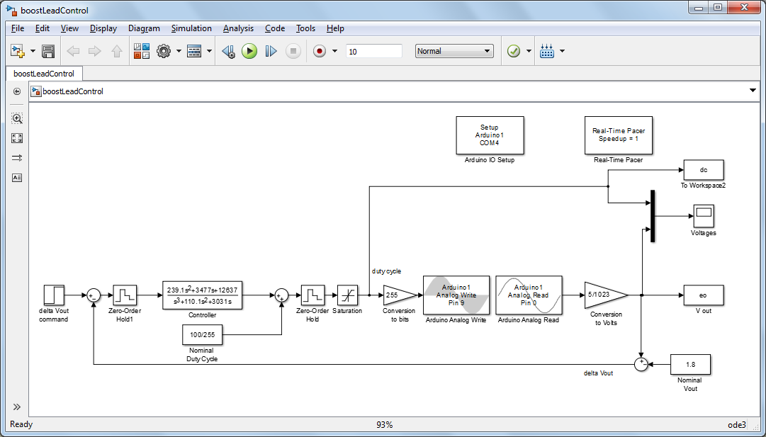
We again set Ts = 0.02 before running the model. This is about as fast as this model can be run. The P control model can actually be run slightly faster because it requires less computation. Running the above model generates the following slightly peculiar output. In the following, we can see that the duty cycle immediately jumps to 100 percent, while the output voltage decays to zero Volts.
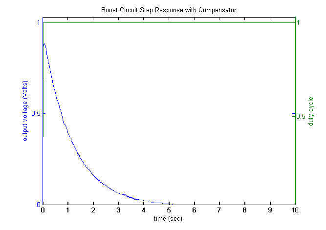
The explanation for this behavior is that the controller is requesting a 100 percent duty cycle which corresponds to the transistor switch being ON 100 percent of the time. When the switch is ON, all of the current from the battery flows through the switch and the load is in effect disconnected from the battery. The initial charge on the capacitor thus decays to zero over time. This behavior is consistent with the non-minimum phase zero in the boost converter transfer function (not included in the simplified model we have been using, see Part (b)) of the activity for more detail). In order to increase the output voltage, the switch is closed to increase the energy stored in the inductor before opening the switch to release that energy to the load. Therefore, when the setpoint voltage request is increased, the output voltage will initially drop since the switch is closed for a longer period of time. Once the energy in the inductor is built up, however, the output voltage will ultimately increase. The initial dip in the output under P control is explained by this phenomenon. In the case of the dynamic compensator, however, the requested duty cycle is too high and the switch stays closed the entire time.
Therefore, we are unable to achieve the speed of response we desire for this boost converter circuit. One solution is to re-design
the dynamic compensator to achieve a slower response by decreasing the gain crossover frequency. Rather than repeating the
entire design process, we will simply reduce the gain  . A value of
  produces a speed of response that is achievable. Specifically, changing the controller to the following and running the Simulink
model again produces the behavior shown below.
(9)
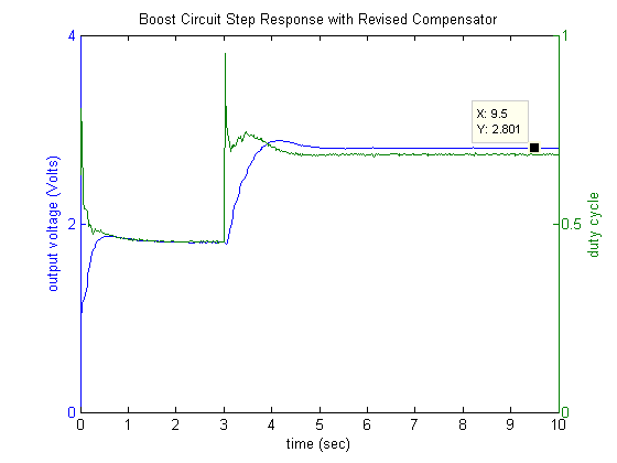
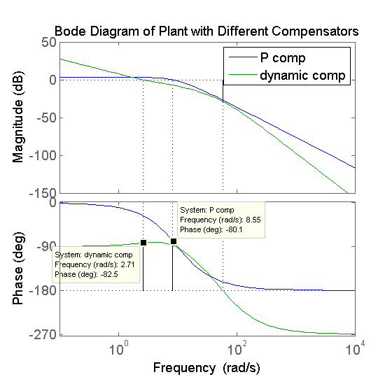
Inspection of the above demonstrates that we are able to achieve a steady-state error of approximately 0 Volts. Comparing the Bode diagrams of the system with P control and the system with revised dynamic compensator can be illustrative in contrasting the resulting behaviors. Specifically, both systems have similar phase margins (~100 degrees) which is in agreement with the fact that both systems exhibit a similar amount of overshoot in response to the step change in voltage request. However, the system with P controller has a significantly higher gain crossover frequency (8.5 rad/sec vs. 2.7 rad/sec). This manifests itself in the faster speed of response of the P controlled system (smaller rise time, smaller peak time). The tradeoff, of course, is that the dynamic compensator is able to achieve zero steady-state error, while the P compensator is not.
Embedded Control
So far in this experiment, the logic for controlling the converter circuit's output voltage has been running in Simulink on a host computer. This was accomplished employing the IO package from the MathWorks which in essence includes a specialized blockset and a program running on board the Arduino for communicating between the board and the host computer running Simulink. The advantage of employing the IO package is that it allows us to communicate with the board in real time with ease. Therefore, we can observe and graph the measured output voltage (and control effort) during the experiment.
An alternative to running the control logic on the host computer is to instead run the control logic on board the Arduino. This is referred to as "embedding" the control on the microprocessor of the Arduino board. This approach has two advantages. One, since the control software does not have to run under an operating system (i.e. Windows, etc.) that has to address many other (higher priority) tasks, the control program can run faster and achieve faster sampling rates. The other advantage is that Arduino board does not need to be physically connected to the host computer. So for example, you can create an intelligent stand-alone device to maintain the voltage supplied to a motor, lighting system, etc. Note that if you want to unplug the Arduino board from the host computer, you will then need to provide an alternative power source (a 9-Volt battery, etc.) for the board. In this activity we so far have been powering the board from the host computer through the USB cable.
In order to embed our control logic on board the Arduino, we will use the standard Arduino Support Package from the MathWorks. More details can be found here. The blockset of this support package is almost identical to those used previously from the IO package. Specifically, the control command (switch on/off) is achieved from a Digital Output block and the output voltage is read via an Analog Input block. The Arduino IO Setup block and the Real-Time Pacer block are no longer necessary, though the model needs to be set to automatically detect the COM port, or must be manually set to the correct COM port. This can be done through the drop-down menu of the model toolbar Tools > Run on Target Hardware > Options.... This is also where the type of board you are using is set. The Scope and To Workspace blocks are no longer employed. The implementation of the revised dynamic compensator with Support Package blockset is shown below and can be downloaded here. This control software can be deployed to the Arduino board by clicking on the icon in the upper righthand corner identified by the red circle below, or by typing Ctrl+B. This automatically builds and compiles the Simulink model into code that runs in real time on board the Arduino. This process of Autocode Generation is becoming very common in industrial practice.
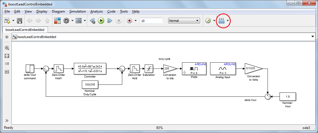
Additionally, if you wish to monitor the performance of your boost converter in real time and have disconnected the Arduino board from the host computer, you then need an alternative means for observing the voltage across the load if you wish to do so. For example, you could employ a voltmeter or an oscilloscope.
Extensions
In this experiment we simply controlled the voltage across a constant resistive load. Alternatively, you could replace the load with a potentiometer and observer the converter's response as you change the setting of the potentiometer. Another option is to replace the load with a device that you actually wish to drive, for example, a DC motor. In this manner the motor can be controlled with a "continuous" voltage, rather than a PWM input.


