


Activity 5 Part (a): Time-Response Analysis of a Boost Converter Circuit

Key Topics: Modeling Electrical Systems, Time-Response Analysis, System Identification, Pulse-Width Modulation
Contents
Equipment needed
- Arduino board (e.g. Uno, Mega 2560, etc.)
- Breadboard
- Battery (AA for example)
- Electronic components (inductor, resistor, capacitor)
- Diode
- Transistor (MOSFET)
- Jumper wires
The system we will be employing in this activity is a type of DC/DC converter called a Boost (Step-Up) Converter. The purpose of a boost converter is to take the voltage supplied by a constant voltage source (e.g. a battery) and output an (approximately) constant higher output voltage. We will implement a couple of very simple (not optimized) versions of a boost converter in order to illustrate its principle of operation. The Arduino board will be used for measuring the output of the circuit via one of the board's Analog Inputs and for controlling the level of the output voltage via one of the board's Digital Outputs. The Arduino board will also communicate the recorded data to Simulink for visualization and analysis.
Purpose
The purpose of this activity is to build intuition regarding the operation of a boost converter circuit. The activity also demonstrates two techniques for modeling and analyzing a simple electrical system. The first approach will model the circuit based on its underlying physics and will compare the predicted time response of the circuit to data taken from a physical implementation of the circuit. The second approach will model the circuit based on experimentally obtained frequency response data and can be found in Part (b) of the activity.
Boost converter principle of operation
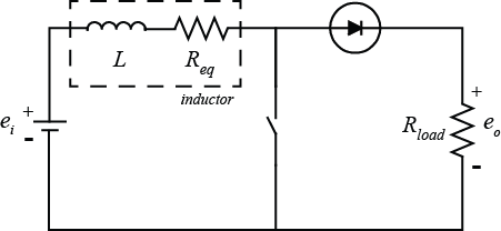
Below is given a simplified version of a boost converter consisting of a DC voltage source  , an inductor
  , a switch, a diode, and a load
  . Here the load is simply a resistor, but it doesn't have to be. In practical applications the load would be a motor, or lighting
system, etc.
. Here the load is simply a resistor, but it doesn't have to be. In practical applications the load would be a motor, or lighting
system, etc.

In the boost circuit, when the switch is closed (shown below) the current from the battery flows primarily through the closed switch since that path is much lower resistance than the parallel path including the load. In practice, the switch will be implemented employing a transistor (MOSFET) and will be controlled from the Arduino board. In this ON state, the inductor in the circuit builds up a store of energy (this enables the voltage across the load to be "boosted" to a higher level than the voltage of the battery). In this state of the shown circuit, negligible current is supplied to the load. In practice, however, a capacitor is included in parallel with the load. This capacitor supplies the load with current when the circuit is in this ON state.

When the switch is opened (shown below), the diode is forward biased and all of the current from the battery flows to the load. Some of the energy that had been stored in the inductor is transferred to the load and the voltage across the load decays.

As the circuit is switched on and off, the output voltage across the load chatters up and down. The output, however, can approximate a constant (DC) voltage by employing a very high switching frequency and by adding the aforementioned capacitor to "filter" the ripple.
Modeling from first principles
At this point we will examine the behavior of the boost circuit described in the previous section with more mathematical rigor. Specifically, we will employ our understanding of the underlying physics of the boost circuit to derive the structure of the system model. We will term this process "modeling from first principles." In this example we employ the variables shown below. In particular, we have added to our model an extra "resistor" that captures the Equivalent Series Resistance (ESR) contributed by the inductor. In this analysis we will treat the transistor as ideal. That is, when the transistor is triggered "on" it will be treated as a short circuit (negligible resistance), and when the transistor is triggered "off" it will be treated as an open circuit (infinite resistance). Similarly, the diode is treated as ideal in that in the forward direction it is treated as having negligible resistance and in the reverse direction it is treated as having infinite resistance.
(Rload) resistance of the load resistor
(Req) equivalent series resistance (ESR) of the inductor
(L) inductance of the inductor
(ei) input voltage (from the battery)
(eo) output voltage
We will begin with the circuit in its ON state and assume that there is initially no current in the circuit ( ). Therefore, all of the current will flow through the switch and since current flows from a higher potential to a lower potential,
the direction of the current will be clockwise as shown below.
). Therefore, all of the current will flow through the switch and since current flows from a higher potential to a lower potential,
the direction of the current will be clockwise as shown below.

Applying Kirchhoff's Voltage Law, the sum of the voltages around the closed loop must equal zero. Thus, the loop law produces the following differential equation which models this boost circuit in its ON state.
(1)
In order to predict the time response of the current in this circuit, we will solve the above differential equation using
the Laplace transform. Taking the Laplace transform of the above gives the following where  is assumed to be a constant equal to
  .
.
(2)
Then solving for  (assuming ), we get the following.
(3)
We can recognize this as a standard first-order step response, or can rearrange the expression by performing a partial fraction expansion.
(4)
Applying the inverse Laplace transform operation to the above, we get the desired time response of the current  .
.
(5)
This response can be identified as a first-order step response with time constant  and DC gain equal to
  , which matches the form of found above. After some time
  , the switch will be opened and all of the current will flow through the load as shown below.

We can again apply Kirchhoff's Voltage Law to model the boost circuit in this OFF state to get the following. For now, we
will assume that the switch occurs at time  (even though it actually occurs at some time ).
(6)
The above differential equation has the same form as in the ON state, but with total resistance  . We can again solve this differential equation employing the Laplace transform, except now we cannot assume the initial current
is zero (
. We can again solve this differential equation employing the Laplace transform, except now we cannot assume the initial current
is zero ( ).
).
(7)
Solving for .
(8)
Examination of the above shows that the first term is the response due to the "input" (the battery voltage) and the second term is the response due to the initial condition. The first term is identical to the circuit in the ON state, except the total resistance is different. Applying the inverse Laplace transform, we arrive at the following.
(9)
Considering that the switch actually occurs at time , the shifted version of the above is the following.
(10)
If we assume that the time of the switch is sufficiently large for the current through the inductor to exceed  , then the current through the inductor will have the following behavior.

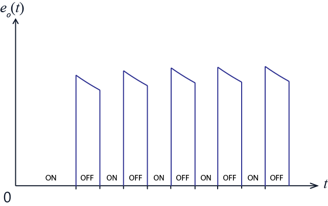
Continuing to switch the boost circuit between its ON and OFF states, the current through the inductor has the following behavior. In practice, the total period (on time plus off time) will be constant and the level of the output voltage will be controlled by varying the duty cycle of the switching (the percent of time the circuit is ON).

When this circuit is in its OFF state, the current through the load  is approximately equal to the current through the inductor. However, when this circuit is in its ON state, almost no current
flows through the load because its resistance is much larger than the resistance through the branch with the switch (the transistor).
Therefore, by applying Ohm's law (
is approximately equal to the current through the inductor. However, when this circuit is in its ON state, almost no current
flows through the load because its resistance is much larger than the resistance through the branch with the switch (the transistor).
Therefore, by applying Ohm's law ( ), we can determine that the output voltage across the load has the following time response.
As mentioned previously, in practice the boost circuit will include a capacitor in parallel with the load to supply the load when the circuit is in its ON state. We will consider the addition of such a capacitor shortly.
Time response experiment
In this experiment we will demonstrate that a physical instantiation of a simple boost circuit will exhibit the behavior predicted by the analysis of the previous section. Specifically, we will use the Arduino board to switch the circuit between its ON and OFF states and to read the output voltage across the load.
Hardware setup
Our simple boost circuit can be implemented on a breadboard and connected to the Arduino board for generating the switching
signal and for recording the output voltage. A schematic of our circuit is shown below. The voltage source () for the circuit is a battery. We will use a AA alkaline battery, but other sizes are acceptable as well. The nominal voltage
of a typical household alkaline battery is 1.5 Volts. This level of voltage allows us to "boost" the output without exceeding
the 5 Volt limit of one of the board's Analog Inputs. We will attempt to size our inductor and load resistor so that the circuit's
response is slow enough that we can reconstruct the shape of the circuit's output waveform with the Arduino board communicating
with the host computer running Simulink. Referring to our prior theoretical analysis, the time constant of the response of
our boost circuit is equal to in the ON state and  in the OFF state. Therefore, in order to keep the circuit response "slow," we wish to use a large inductor while keeping
the resistances relatively small. In this experiment we will use a 1 H inductor with an approximate equivalent series resistance
of 40
in the OFF state. Therefore, in order to keep the circuit response "slow," we wish to use a large inductor while keeping
the resistances relatively small. In this experiment we will use a 1 H inductor with an approximate equivalent series resistance
of 40  that was relatively inexpensive to purchase. The load resistance is chosen to be approximately 60 . Since our circuit is low power with relatively slow switching, we don't need to be too particular about our choice of transistor
or diode. One possible choice of power MOSFET is the IRF1520 whose datasheet can be found here. The orientation of the Gate, Source, and Drain pins are identified in the figure below. For our diode, we will employ the
general purpose 1N4007 whose datasheet can be found here.
that was relatively inexpensive to purchase. The load resistance is chosen to be approximately 60 . Since our circuit is low power with relatively slow switching, we don't need to be too particular about our choice of transistor
or diode. One possible choice of power MOSFET is the IRF1520 whose datasheet can be found here. The orientation of the Gate, Source, and Drain pins are identified in the figure below. For our diode, we will employ the
general purpose 1N4007 whose datasheet can be found here.

The setup of the boost circuit and its connection to the Arduino board is shown below. The color band on the diode indicates its cathode. The Gate, Source, and Drain pins of the MOSFET can be deduced from its orientation in the given figure.

Software setup
In this experiment, we will employ Simulink to control the switching of the transistor, to read the output voltage data from the board, and to plot the data in real time. In particular, we will employ the IO package from the MathWorks. For details on how to use the IO package, refer to the following link. The Simulink model we will use is shown below and can be downloaded here, where you may need to change the port to which the Arduino board is connected (the port is COM3 in this case).
The Pulse Generator block toggles between 0 and 1 and is connected to the Digital Write Block to switch the transistor between
its OFF state and its ON state, respectively. Referring to our previous analysis with the components identified above ( H,
H,  ,
,  ), the time constant of our circuit is approximately
  seconds in its ON state and
  seconds in its OFF state. As it takes approximately 4 time constants for a first-order step response to reach 98 percent
of its steady-state value, we set up the Pulse Generator block to have a period of 0.2 seconds with a duty cycle of 50 percent.
In other words, the circuit is ON for 0.1 seconds and OFF for 0.1 seconds. This amount of time is sufficiently long for the
output to range between close to its minimum and close to its maximum. As the gate of the MOSFET is triggered from Digital
Output 9, the Digital Write block needs to be set to the corresponding pin. Specifically, double-clicking on the block allows
us to set the Pin to 9 from the drop-down menu. We also will set the Sample Time. In order to clearly capture the transient response of the circuit, we will choose our sampling time to be 0.01 seconds (2.5
times faster than the OFF time constant). This sampling period is around the limit of what the IO package can achieve running
under the Windows operating system. If you need to increase the sample time to 0.02 seconds, you should still achieve reasonably
clear results. The downloadable model included above defines all sample times as Ts (or left as "-1"). Therefore, before you run this model you must define the variable Ts in the MATLAB workspace by typing Ts = 0.01; at the command line. Since the output voltage is read on Analog Input AO, the Analog Read block needs to be set to that channel.
This is again achieved by double-clicking on the block and setting the Pin to 0 from the drop-down menu. This block is also set to have a sample time of Ts.
seconds in its OFF state. As it takes approximately 4 time constants for a first-order step response to reach 98 percent
of its steady-state value, we set up the Pulse Generator block to have a period of 0.2 seconds with a duty cycle of 50 percent.
In other words, the circuit is ON for 0.1 seconds and OFF for 0.1 seconds. This amount of time is sufficiently long for the
output to range between close to its minimum and close to its maximum. As the gate of the MOSFET is triggered from Digital
Output 9, the Digital Write block needs to be set to the corresponding pin. Specifically, double-clicking on the block allows
us to set the Pin to 9 from the drop-down menu. We also will set the Sample Time. In order to clearly capture the transient response of the circuit, we will choose our sampling time to be 0.01 seconds (2.5
times faster than the OFF time constant). This sampling period is around the limit of what the IO package can achieve running
under the Windows operating system. If you need to increase the sample time to 0.02 seconds, you should still achieve reasonably
clear results. The downloadable model included above defines all sample times as Ts (or left as "-1"). Therefore, before you run this model you must define the variable Ts in the MATLAB workspace by typing Ts = 0.01; at the command line. Since the output voltage is read on Analog Input AO, the Analog Read block needs to be set to that channel.
This is again achieved by double-clicking on the block and setting the Pin to 0 from the drop-down menu. This block is also set to have a sample time of Ts.
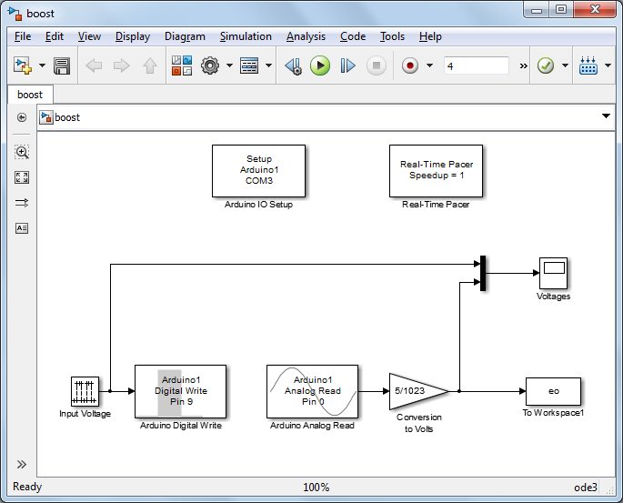
The Gain block is included to convert the data into units of Volts (by multiplying the data by 5/1023). This conversion can
be understood by recognizing that the Arduino Board employs a 10-bit analog-to-digital converter, which means (for the default)
that an Analog Input channel reads a voltage between 0 and 5 V and slices that range into  pieces. Therefore, 0 corresponds to 0 V and 1023 corresponds to 5 V. The given Simulink model then plots the recorded output
voltage on a scope and also writes the output data to the MATLAB workspace for further analysis. The Arduino Digital Write
block, the Arduino Analog Read block, the Arduino IO Setup block, and the Real-Time Pacer block are all part of the IO package.
The remaining blocks are part of the standard Simulink library, specifically, they can be found under the Math, Sources, and
Sinks libraries.
pieces. Therefore, 0 corresponds to 0 V and 1023 corresponds to 5 V. The given Simulink model then plots the recorded output
voltage on a scope and also writes the output data to the MATLAB workspace for further analysis. The Arduino Digital Write
block, the Arduino Analog Read block, the Arduino IO Setup block, and the Real-Time Pacer block are all part of the IO package.
The remaining blocks are part of the standard Simulink library, specifically, they can be found under the Math, Sources, and
Sinks libraries.
Running the above model for 2 seconds generates the figure shown below of output voltage versus time. The character of the displayed response matches what we predicted, the voltage across the load decays exponentially when the circuit is in its OFF state and the voltage (current) drops to near zero when the circuit is in its ON state.

Let's look at how the range of the output voltage compares to our expectations. Employing Ohm's law and our previous analysis,
the maximum voltage across the load is predicted to be  Volts (where
  Volts in this case). Considering that the output signal is only sampled once every 0.01 seconds, it is likely the recorded
data misses the peak voltage (if it occurs between samples). Furthermore, our analysis made several simplifying assumptions.
Therefore, the data shown above matches our expectations reasonably well. Again employing Ohm's law and our previous analysis,
the minimum voltage across the load when the circuit is in its OFF state is predicted to be
Volts in this case). Considering that the output signal is only sampled once every 0.01 seconds, it is likely the recorded
data misses the peak voltage (if it occurs between samples). Furthermore, our analysis made several simplifying assumptions.
Therefore, the data shown above matches our expectations reasonably well. Again employing Ohm's law and our previous analysis,
the minimum voltage across the load when the circuit is in its OFF state is predicted to be  Volts. The actual data demonstrates a limiting output voltage more in the neighborhood of 0.54 Volts, which while not exactly
equal, is not bad considering all of the simplifications we made in our analysis. Specifically, we treated the transistor,
the diode, and the input and output channels of the board as ideal, which they of course are not.
Volts. The actual data demonstrates a limiting output voltage more in the neighborhood of 0.54 Volts, which while not exactly
equal, is not bad considering all of the simplifications we made in our analysis. Specifically, we treated the transistor,
the diode, and the input and output channels of the board as ideal, which they of course are not.
The time constant of the circuit in the OFF state indicated by the above data also seems to be quite similar to the prediction of 0.01 seconds (though a bit larger).
Time response with capacitor
As mentioned previously, in order to keep the output voltage from dropping all the way to zero when the boost circuit is in its ON state, one typically adds a capacitor in parallel with the load as shown in the following. When this configuration of the circuit is in its OFF state, the current that previously went entirely to the load is split between the load and the capacitor. The current sent to the capacitor builds up charge on the capacitor. When the circuit then switches to the ON state and all of the current from the battery flows through the branch with the transistor, then the charge built up on the capacitor is released to the load.

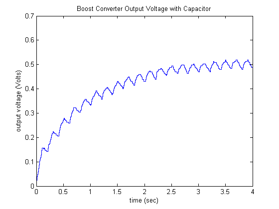
Employing the same Simulink model from above and a 22000  capacitor in parallel with the load, the voltage generated across the load is shown below. A relatively large capacitor is
chosen so that the dynamics are slow enough that the capacitor does not completely discharge when the circuit is in its ON
state. When the capacitor does not completely discharge, the converter is said to be in "continuous conduction mode." The
relatively large size of the capacitor means that it takes a while for the circuit to reach steady state (for the capacitor
to charge up) as can be seen in the figure below.
capacitor in parallel with the load, the voltage generated across the load is shown below. A relatively large capacitor is
chosen so that the dynamics are slow enough that the capacitor does not completely discharge when the circuit is in its ON
state. When the capacitor does not completely discharge, the converter is said to be in "continuous conduction mode." The
relatively large size of the capacitor means that it takes a while for the circuit to reach steady state (for the capacitor
to charge up) as can be seen in the figure below.
We can analyze this boost circuit from first principles to again better understand the dynamics of the circuit. First we will
consider the circuit in its OFF state with no initial current ( ). The fact that the initial conditions are zero means that we can analyze the circuit in the Laplace domain, that is, employing
complex impedances. Considering each of the circuit elements in terms of their complex impedances, the circuit in its OFF
state can be considered as follows.
). The fact that the initial conditions are zero means that we can analyze the circuit in the Laplace domain, that is, employing
complex impedances. Considering each of the circuit elements in terms of their complex impedances, the circuit in its OFF
state can be considered as follows.
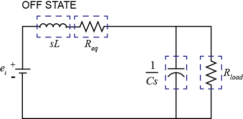
Examining the above, we can combine the impedances of the inductor and its equivalent series resistance using the fact that
the impedances of components in series add,  . We can also combine the impedances of the capacitor and the load resistance in the following manner since these two components
are in parallel.
. We can also combine the impedances of the capacitor and the load resistance in the following manner since these two components
are in parallel.
(11)![$$ Z_2(s) = \left[ \frac{1}{1/Cs} + \frac{1}{R_{load}} \right]^{-1} =
\frac{R_{load}}{R_{load}Cs+1} $$](Content/Activities/html/Activities_BoostcircuitA_eq28241.png)
With these reductions, we can think of the boost converter in this state as something of a voltage divider.

Therefore, we can generate the following transfer function for the circuit in this state for an input of and an output of  using the fact that is the voltage across both
  and
and  which are in series and is the voltage across .
(12)
Performing some algebra, we generate the following second-order model.
(13)
Considering the values of the various components in our boost circuit, we can determine the poles of this transfer function using the following MATLAB commands.
Rload = 60;
Req = 40;
L = 1;
C = 22000*10^-6;
s = tf('s');
P = Rload/(L*Rload*C*s^2 + (Req*Rload*C + L)*s + Req + Rload)
pole(P)
P =

            60
  -----------------------
  1.32 s^2 + 53.8 s + 100

Continuous-time transfer function.

ans =
  -38.8053
   -1.9522
Based on the above, we can see that the circuit in this mode is overdamped since it has two real poles. Furthermore, since
the pole at  is about 20 time smaller than the other pole, it will dominate the character of the response and the circuit will behave
approximately as a first-order system with time constant
is about 20 time smaller than the other pole, it will dominate the character of the response and the circuit will behave
approximately as a first-order system with time constant  . Considering the input voltage from the battery as a step input when the battery is initially connected to the circuit, we
can envision what the output voltage response looks like.
. Considering the input voltage from the battery as a step input when the battery is initially connected to the circuit, we
can envision what the output voltage response looks like.
When the boost converter is switched ON, the charge built up on the capacitor is released to the load and we can evaluate the output voltage response based on the following circuit. Note, in this ON state the energy from the battery still goes to increasing the energy stored in the inductor.

Examining the circuit containing the capacitor and the load, we can apply Kirchhoff's Voltage Law to model the circuit as shown below.
(14)
We can solve this integro-differential equation applying the Laplace transform to arrive at the expression shown below. Note
that the integral has an initial value since the capacitor is initially charged. For convenience, we will assume the switch
to the ON state takes place at .
(15)![$$ I_R(s) R_{load} + \frac{1}{Cs}\left[ I_R(s) + \int i_R\ dt\vert_{t =
0} \right] = 0 $$](Content/Activities/html/Activities_BoostcircuitA_eq12034.png)
Using the fact that the value of the integral at the time of the switch is the negative of the initial charge on the capacitor
 (current is the time derivative of charge), we can solve for
  as follows.
(16)
Recalling the definition of capacitance, we have that  . Therefore, we have the following.
(17)
Applying Ohm's law ( ) and the inverse Laplace transform, we then have the time response of the output voltage when the switch is turned ON.
(18)![$$ e_o(t) = \mathcal{L}^{-1} \left[ \frac{R_{load}C}{R_{Load}Cs + 1}e_o(0) \right] = e_o(0)e^{-t/R_{load}C},\ t \geq 0 $$](Content/Activities/html/Activities_BoostcircuitA_eq88176.png)
In other words, when the switch is turned ON the output voltage decays exponentially from its initial value with time constant
 , which is 1.32 seconds in this case (slower, but similar to the time constant in the OFF state). This analysis of the boost
converter's response with capacitor in its ON and OFF states is consistent with the data recorded and depicted at the beginning
of this section.
, which is 1.32 seconds in this case (slower, but similar to the time constant in the OFF state). This analysis of the boost
converter's response with capacitor in its ON and OFF states is consistent with the data recorded and depicted at the beginning
of this section.
In practice, it is desired that the response of the boost converter be faster and smoother than the example circuit we have presented here. This is achieved principally by choosing different circuit components (a smaller capacitor for example) and by employing a PWM input with significantly higher frequency. Employing a higher frequency PWM input makes the response smoother by virtue of the fact that there is less time in the ON and OFF states for the circuit output to decay and rise, respectively. We will examine the response of a converter under these conditions in Part (b) of this activity.
Extensions
Some extensions to this activity would be to experiment with different circuit components to see what kind of performance can be achieved. It could also be interesting to examine other types of DC/DC converters, such as the buck converter and the buck-boost converter.
