


Activity 2 Part (a): Time-Response of an Inductor–Resistor–Capacitor (LRC) Circuit
Key Topics: Modeling Electrical Systems, Underdamped Second-Order Systems, System Identification
Contents
Equipment needed
- Arduino board (e.g. Uno, Mega, etc.)
- Breadboard
- Battery (AA for example)
- Electronic components (inductor, resistor, capacitor)
- Switch (pushbutton, or can employ a transistor)
- Jumper wires
The system we will be employing in this activity is a simple electrical circuit consisting of an inductor (L), a resistor (R), and a capacitor (C) in series. The Arduino board will be used for measuring the output of this LRC circuit and possibly for triggering the input to the circuit. The input to the circuit will be a voltage step, supplied by a battery through a push-button switch, applied across all three components in series. The output of the circuit will be the voltage across the capacitor, which will be read via one of the board's Analog Inputs. This data is then fed to Simulink for visualization and for comparison to our resulting simulation model output.
Purpose
The purpose of this activity is to demonstrate how to model a simple electrical system. Specifically, a first-principles approach based on the underlying physics of the circuit will be employed. The associated experiment is employed to determine the accuracy of the resulting model and to demonstrate how the individual circuit components affect the response. This activity also provides a physical example of the common class of (underdamped) second-order systems.
Modeling from first principles
First we will employ our understanding of the underlying physics of the LRC circuit to derive the structure of the system model. We will term this process "modeling from first principles." In this example, we employ the variables shown below. In textbooks, the various components of a circuit are often treated as "ideal." It is important to know when such idealized models can be employed (and when they can't). In this experiment we will include the resistance contributed by our inductor (termed the inductor's equivalent series resistance (ESR)) because it will turn out to be significant. Specifically, we will employ a rather large inductor in order to achieve an underdamped step response. Such large inductors commonly have significant ESR, though lower ESR inductors exist if you are willing to spend more money! Capacitors also contribute resistance, but the associated ESR won't be significant for the size of capacitor we will ultimately employ. Later we will also briefly discuss the simplification of treating a transistor as an ideal switch.
(R) resistance of the resistor
(L) inductance of the inductor
(Req) equivalent series resistance (ESR) of the inductor
(C) capacitance of the capacitor
(ei) input voltage
(eo) output voltage

To begin, we assume a direction for the current and then apply Kirchoff’s Voltage Law (loop law). Current flows from a higher potential to a lower potential, therefore, the direction of the current will be clockwise in this case (shown below).
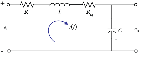
The loop law states that the sum of voltages around a closed loop must equal zero. Thus, the loop law produces the following governing equation for the circuit.
(1)
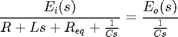
An alternative to an integro-differential equation model of a dynamic system is the transfer function. The transfer function captures the input/output behavior of a system and is derived by first taking the Laplace transform
of a given integro-differential equation, while assuming zero initial conditions ( ).
).
(2)
Next we must perform some algebra to rearrange the above into the form of its output divided by its input. In this case, our
input is  and our output is
  . Therefore, we must eliminate current
  from the above since it is neither an input nor an output, and we must introduce the output into the above equation. Solving the above equation for we arrive at the following.
(3)
Next we can recognize that the output voltage (across the capacitor) is  . Taking the Laplace transform and again solving for , we arrive at the following.
(4)
Setting the two previous equations equal to one another, we can eliminate .
(5)
Then re-arranging into the desired form of output divided by input, we produce the resulting transfer function model.
(6)
Recognizing the above as a second-order system, we can manipulate the transfer function so that it has the standard, canonical form shown below.
(7)
In this form we can see by inspection how the parameters of the circuit affect its transient response (though not the steady-state response). Specifically, the circuit components affect the parameters of the canonical second-order system in the following manner.
(8)
(9)
(10)
These relations then relate to the characteristics of an underdamped second-order step response. Note, the DC gain is 1 no matter the choice of component values.
System identification experiment
In this experiment we will record the output voltage of the LRC circuit for a step in input voltage. We then will compare the data to the response predicted by the first-principles derived model we created previously.
Hardware setup
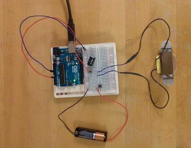
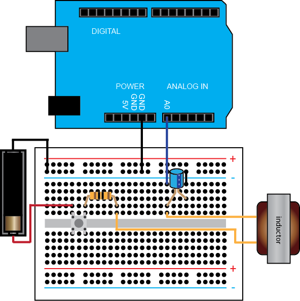
Our simple LRC circuit can be implemented on a breadboard and connected to the Arduino board for recording the output voltage. There are different techniques for generating our voltage "step" input. We will specifically employ a battery as our voltage source with a push-button switch. The act of completing the circuit with the switch is equivalent to applying a step input. Driving the circuit with one of the Arduino board's Digital Outputs is problematic for a couple of reasons. For one, the Digital Output from the board provides a 5-Volt step input. This means that if the circuit is underdamped, then the output voltage will overshoot 5 Volts since the DC gain is 1. This overshoot would cause the output voltage to exceed the allowed range of the Analog Input. This could be alleviated by employing a different circuit configuration, but there is another issue. Switching the inductive load can make it difficult for the Digital Output to generate a true step, since the voltage tends to get pulled down. The same issue can arise with the 3.3 Volt source on the board. Employing a battery (AA for example) with a switch avoids these issues. The nominal voltage for most alkaline household batteries (AAA, AA, D, etc.) is 1.5 Volts.

The setup of the LRC circuit and its connection to the Arduino board is shown below. The biggest challenge to achieving an
underdamped response ( ) that is not too fast for the Arduino board to sample (
 not too large) is to employ an inductor with sufficient inductance but not too much ESR. We will employ a 1
  inductor with 40
  ESR that was relatively inexpensive to purchase. We will also employ a 510
  capacitor and a 10 resistor, though this resistor is not necessary (make sure it is not too large). These components provide a damping ratio
of
capacitor and a 10 resistor, though this resistor is not necessary (make sure it is not too large). These components provide a damping ratio
of  . One thing to note is that if you employ an electrolytic capacitor, its orientation matters. Specifically, if your capacitor
has legs of different lengths and one leg is marked by a negative sign, then you have an electrolytic capacitor. Orient an
electrolytic capacitor so that the leg marked by the negative sign connects to the lower potential part of the circuit (ground
in this case). The Arduino board is employed to acquire the output voltage data from the circuit (via an Analog Input) and
communicates the data to Simulink.
. One thing to note is that if you employ an electrolytic capacitor, its orientation matters. Specifically, if your capacitor
has legs of different lengths and one leg is marked by a negative sign, then you have an electrolytic capacitor. Orient an
electrolytic capacitor so that the leg marked by the negative sign connects to the lower potential part of the circuit (ground
in this case). The Arduino board is employed to acquire the output voltage data from the circuit (via an Analog Input) and
communicates the data to Simulink.
Software setup
In this experiment, we will employ Simulink to read the data from the board and to plot the data in real time. In particular, we will employ the IO package from the MathWorks. For details on how to use the IO package, refer to the following link. The Simulink model we will use is shown below and can be downloaded here, where you may need to change the port to which the Arduino board is connected (the port is COM3 in this case).
As shown below, this Simulink model simply reads the output voltage of the LRC circuit. Specifically, the Arduino Analog Read
block reads the output voltage data via the Analog Input A0 on the board. Double-clicking on the block allows us to set the
Pin to 0 from the drop-down menu. We also will set the Sample Time. Referring to the earlier equations and the nominal component values,  rad/sec. Since , this means that
  rad/sec. Therefore, we will expect a peak time for our step response of approximately
  seconds. In order to clearly capture the transient response of the circuit, we will choose our sampling time to be 0.01 seconds.
This sampling period is close to the limit of what the IO package can achieve running under the Windows operating system,
but is necessary to reconstruct this particular step response accurately. The downloadable model included above defines all
sample times as Ts (or left as "-1"). Therefore, before you run this model you must define the variable Ts in the MATLAB workspace by typing Ts = 0.01; at the command line.
seconds. In order to clearly capture the transient response of the circuit, we will choose our sampling time to be 0.01 seconds.
This sampling period is close to the limit of what the IO package can achieve running under the Windows operating system,
but is necessary to reconstruct this particular step response accurately. The downloadable model included above defines all
sample times as Ts (or left as "-1"). Therefore, before you run this model you must define the variable Ts in the MATLAB workspace by typing Ts = 0.01; at the command line.
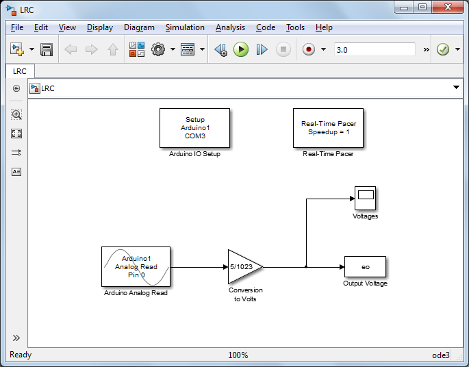
The other blocks in the model can also be set to have a sample time of Ts. The Gain block is included to convert the data into units of Volts (by multiplying the data by 5/1023). This conversion
can be understood by recognizing that the Arduino Board employs a 10-bit analog-to-digital converter, which means (for the
default) that an Analog Input channel reads a voltage between 0 and 5 V and slices that range into  pieces. Therefore, 0 corresponds to 0 V and 1023 corresponds to 5 V. The given Simulink model then plots the recorded output
voltage on a scope and also writes the output data to the MATLAB workspace for further analysis. The Arduino Analog Read block,
the Arduino IO Setup block, and the Real-Time Pacer block are all part of the IO package. The remaining blocks are part of
the standard Simulink library, specifically, they can be found under the Math and Sinks libraries.
pieces. Therefore, 0 corresponds to 0 V and 1023 corresponds to 5 V. The given Simulink model then plots the recorded output
voltage on a scope and also writes the output data to the MATLAB workspace for further analysis. The Arduino Analog Read block,
the Arduino IO Setup block, and the Real-Time Pacer block are all part of the IO package. The remaining blocks are part of
the standard Simulink library, specifically, they can be found under the Math and Sinks libraries.
Recall that the "step input" to our LRC circuit is generated employing a push button as described earlier. Therefore, once you begin the model running, you will need to press the push button to cause the input voltage to step. One such set of data is shown below. Note that this data is for the case that the capacitor initially has no charge. If you are performing successive runs and wish to begin with an initial output voltage of zero, then you will need to discharge the capacitor before performing a run. This can be done by simply shorting (placing a wire between) the two legs of the capacitor.

In the next section we will compare this data to the response predicted by our previously derived first-principle's model.
Model validation
At this point we will now use the MATLAB command step to generate the step response predicted by the first-principles model generated earlier. The transfer function version of this model is repeated below.
(11)
In order to facilitate the comparison between the predicted and collected data, we will shift the recorded data so that the
step occurs at time  seconds (step appears to occur at time equal to 1.22 seconds). Furthermore, we will scale the predicted response to account
for the fact that the input is not a unit step. Based on the steady-state value of the recorded data, it appears the battery's
voltage is approximately 1.53 Volts (the battery voltage in this example is negligibly affected by changes in the load).
seconds (step appears to occur at time equal to 1.22 seconds). Furthermore, we will scale the predicted response to account
for the fact that the input is not a unit step. Based on the steady-state value of the recorded data, it appears the battery's
voltage is approximately 1.53 Volts (the battery voltage in this example is negligibly affected by changes in the load).
Applying the following MATLAB commands, where the output of our Simulink model from above eo is saved as a time series, will generate the plot shown below.
         s = tf('s');
         R = 10;                                           % resistor resistance
         Req = 40;                                         % inductor equivalent series resistance (ESR)
         L = 1;                                            % inductor inductance
         C = 510*10^-6;                                    % capacitor capacitance
         ei = 1.53;                                        % battery voltage
         tstep = 1.22;                                     % time step occurred
         G = 1/(C*L*s^2 + C*(R+Req)*s + 1);                % model transfer function
         [y,t] = step(G*ei,0.5);                           % model step response with battery voltage scaling
         plot(t,y)
         hold
         plot(eo.Time(100*tstep:100*tstep+50)-tstep,eo.Data(100*tstep:100*tstep+50),'r:') % experimental data
         xlabel('time (sec)')
         ylabel('output voltage (Volts)')
         title('LRC Circuit Step Response')
         legend('model','experiment','Location','SouthEast')
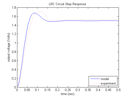
Examining the above, the predicted and actual responses are similar, though not exactly the same. The primary contributor
to this is likely variation in the component values from their nominal labeled values. Since the actual peak time is greater
than predicted, this indicates that is smaller than predicted since  . Since the overshoot is slightly larger than predicted, that would indicate
  is smaller than anticipated. Taken together, this also indicates
  is smaller than anticipated since
  . From prior analysis, we have the following.
(12)
(13)
Therefore, it is possible that the product of the capacitor's capacitance and the inductor's inductance is larger than indicated
(explaining ). It is also possible that inductance is larger than anticipated, or that the resistances and capacitance are smaller than
predicted (explaining ).
Other factors besides the variation in the system component values could also explain the difference between the observed response and that predicted by the model. Specifically unmodeled dynamics, variation in sampling time, and the input not being a perfect step could contribute. One significant source of unmodeled dynamics is the loading effect of the channel that is reading the output voltage. In other words, the channel itself does not have infinite impedance.
Alternative implementation
In the above experiment we generated our "step" input using a battery and a push-button switch. If you would like more control over the timing of this input step, you can instead use a Digital Output from the Arduino board to trigger the step using a transistor as a switch.
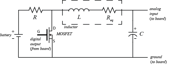
A circuit for achieving this implementation is shown below that employs a MOSFET transistor where the pins for the Gate, Source,
and Drain are identified. One possible choice of power MOSFET is the IRF1520 whose datasheet can be found here. The circuit is set up this way for two reasons. For one, it is desirable to connect the source S to ground because that
limits the level of voltage needed to trigger the transistor at the gate G. In other words, the potential difference between
the gate G and the source S needs to cross a threshold to fully switch the transistor "ON" (to create a low resistance connection
between the drain D and the source S). The transistor we employ here has a threshold between 2 and 4 Volts. The other reason
is that in this configuration when the transistor is "ON" and behaving as a closed switch, then there is little current flowing
to the capacitor so that it does not build up much charge. For the transistor we employ here, in the "ON" state it has a resistance
between the drain and source of approximately 0.2 . This resistance is much smaller than the ESR of the inductor (overall impedance much smaller too), therefore, most of the
current will flow through the transistor and not the path with the capacitor. For example, we could generate a step response
like we did with the push button in the following manner. First we set the Digital Output from the Arduino board high (5 Volts)
to close the transistor switch. This causes most of the battery current to flow through the path with the transistor and will
allow the capacitor to discharge if it has charge built up on it. We can then set the Digital Output from the board low (0
Volts) to open the transistor switch. When that occurs, most all of the current from the battery flows through the series
LRC circuit and it is as if the input voltage from the battery has been stepped.
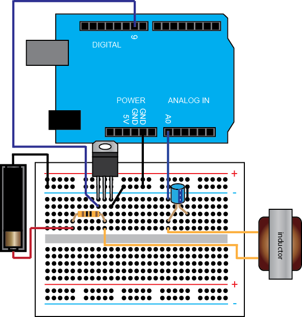
A wiring example showing the connections to the Arduino Board and the orientation of the MOSFET is shown below.
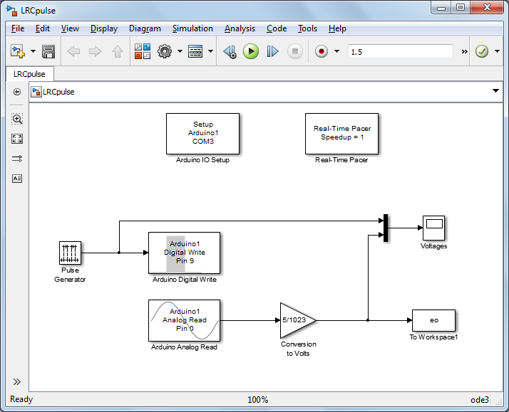
In order to generate the Digital Output from the Arduino board, the Simulink model created earlier needs to be modified to include a Digital Write block and a Pulse Generator block as shown below. The Digital Write block is set to output on Pin 9, while the Pulse Generator block is set to output 1 for the first second of the run (in order to discharge the capacitor) then the output switches to 0 which causes the current to the LRC circuit to "step." The model shown below can be can be downloaded here.
The result of running this model is shown below where the capacitor initially has charge built up because the transistor switch was "open" while the MOSFET was not being triggered.

Executing the following MATLAB code in the command window will generate the step response predicted by our first principles model and plot it next to the actual experimental data, where the output of our Simulink model from above, eo, is saved as a time series.
         s = tf('s');
         R = 10;                                           % resistor resistance
         Req = 40;                                         % inductor equivalent series resistance (ESR)
         L = 1;                                            % inductor inductance
         C = 510*10^-6;                                    % capacitor capacitance
         ei = 1.5;                                         % battery voltage
         G = 1/(C*L*s^2 + C*(R+Req)*s + 1);                % model transfer function
         [y,t] = step(G*ei,0.5);                           % model step response with battery voltage scaling
         plot(t,y)
         hold
         plot(eo.Time(101:151)-1.01,eo.Data(101:151),'r:') % experimental data
         xlabel('time (sec)')
         ylabel('output voltage (Volts)')
         title('LRC Circuit Step Response')
         legend('model','experiment','Location','SouthEast')

Examination of the above demonstrates a similar level of agreement between the experiment and the prediction as was achieved with the push-button switch. More accurate measurement of the circuit components would achieve better agreement between the model and the experimental data.
Extensions
Alternate LRC circuits can be examined to investigate the modeling of circuits that are not canonical first-order or second-order systems. Specifically, the effect of zeros and higher-order poles can be examined. One can also employ variable resistors (potentiometers) or variable capacitors to examine the effect of different parameters. In Part (b) of this activity, an RC circuit is added in series with the LRC circuit examined here.
